Wide Bandgap Semiconductors in 2026: GaN and SiC Move from Niche to Mainstream
Table of Contents
⚡ Sourcing Summary
Wide-bandgap (WBG) semiconductors like Gallium Nitride (GaN) and Silicon Carbide (SiC) are transforming high-efficiency power designs in 2026. Sourcing these devices requires strict verification of dynamic on-resistance and thermal dissipation limits. OEMs should establish dual-sourced pipelines to prevent supply disruptions.
The transition from silicon to wide bandgap (WBG) semiconductors—primarily Gallium Nitride (GaN) and Silicon Carbide (SiC)—represents the most significant shift in power electronics since the IGBT displaced bipolar junction transistors three decades ago. In 2026, this transition has reached an inflection point: WBG devices have moved decisively beyond early-adopter niches into volume production across automotive, industrial, and data center applications.
The Physics Advantage
At the device physics level, both GaN and SiC offer fundamental advantages over silicon for power switching applications. Their wider bandgap (3.4 eV for GaN, 3.3 eV for 4H-SiC, versus 1.1 eV for silicon) enables higher breakdown voltages, while higher electron mobility translates to faster switching speeds with lower conduction and switching losses.
The practical implications are transformative:
-
SiC MOSFETs operating at 1200V and above can switch at frequencies that would destroy equivalent silicon IGBTs while delivering 50-70% lower switching losses. In traction inverters, this translates directly to extended EV range.
-
GaN HEMTs (High Electron Mobility Transistors) achieve switching frequencies in the megahertz range at 650V, enabling power supplies that are one-third the size and weight of silicon equivalents. A 3 kW GaN-based server PSU in 2026 fits in a 1U form factor that would have required 2U with silicon.
-
Reverse Recovery Charge (Qrr) is effectively zero in GaN HEMTs and near-zero in SiC Schottky diodes, eliminating a major source of EMI and switching loss that has plagued silicon power converters for decades.
The 2026 Market Landscape
The WBG semiconductor market has grown at a 28% CAGR from 2023 to 2026, reaching approximately $12 billion according to Yole Group’s Q1 2026 Power Semiconductor Market Monitor. SiC dominates in revenue terms (roughly 70% of the WBG market) due to its entrenched position in automotive traction inverters, while GaN is growing faster in unit volume, driven by consumer power adapters, data center power supplies, and LiDAR applications.
Silicon Carbide: The Automotive Workhorse
SiC’s dominance in automotive is now absolute for premium EVs. Tesla’s early adoption of SiC MOSFETs in the Model 3 inverter (2017) proved the technology’s viability. By 2026, essentially every new EV platform with a range exceeding 300 miles uses SiC in the main traction inverter, and the technology is rapidly filtering down to mid-range platforms.
The supply chain has expanded dramatically to meet demand:
-
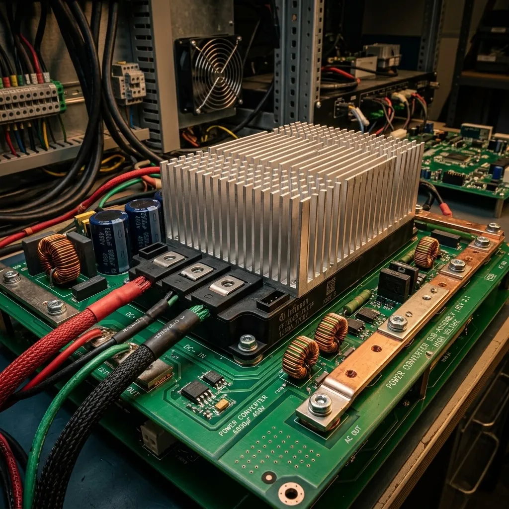
STMicroelectronics has invested over €5 billion in SiC substrate and device manufacturing capacity, including its fully integrated Catania campus, which produces 200mm SiC wafers at volume—a milestone that has reduced substrate costs by approximately 40% compared to 150mm production.
-
Wolfspeed’s Siler City, North Carolina 200mm SiC fab reached full production capacity in early 2026, capable of producing 600,000 wafers annually for both discrete devices and bare die.
-
ON Semiconductor has vertically integrated from SiC crystal growth through module assembly, with its Hudson, New Hampshire and Roznov, Czech Republic facilities handling the entire value chain.
-
Chinese SiC capacity has grown explosively, with over 40 domestic SiC substrate and epi suppliers now operating. Sanan, TankeBlue, and SICC collectively represent approximately 25% of global SiC substrate capacity, though yields and defect densities still lag behind Wolfspeed and Coherent (formerly II-VI).
The bottleneck has shifted from substrate availability to module packaging. SiC dies capable of operating at 200°C junction temperatures require advanced packaging solutions—silver sintering for die attach, advanced ceramic substrates (Si3N4 replacing Al2O3), and copper ribbon bonding replacing aluminum wire bonds. Companies that have mastered high-reliability SiC packaging, such as Semikron-Danfoss and Infineon, command significant premiums in the automotive qualification pipeline.
Gallium Nitride: From USB Chargers to Data Centers
GaN’s trajectory has been different from SiC’s. While SiC attacked the high-power, high-voltage end of the market, GaN initially found its beachhead in low-power consumer applications—USB-C chargers, where its high-frequency operation enabled dramatic size reductions.
In 2026, GaN has pushed decisively into higher power levels:
-
Data Center Power Supplies: The Open Compute Project (OCP) 3.0 specification has essentially mandated GaN-based power supplies for new hyperscale data center deployments. A 3.2 kW GaN PSU operating at 1 MHz achieves 98.5% peak efficiency (Titanium Plus), saving approximately 15 watts of losses per unit compared to the best silicon designs. Across a 100 MW data center, this translates to roughly 1.5 MW of avoided power losses.
-
AI Server Power Delivery: The power demands of AI accelerators have accelerated GaN adoption. NVIDIA’s H200 and B100 GPU modules require 48V bus architectures with 48V-to-1V direct conversion at 1000A+ current levels. GaN-based intermediate bus converters (IBCs) and voltage regulator modules (VRMs) are the only practical solution for achieving the required power density and transient response.
-
Automotive On-Board Chargers (OBCs): While SiC dominates the traction inverter, GaN is gaining in OBC applications where bidirectional 11-22 kW chargers benefit from GaN’s superior light-load efficiency and ability to operate at very high frequencies, reducing magnetics size.
-
LiDAR and Sensing: GaN’s ability to generate nanosecond-duration laser pulses at high repetition rates has made it the dominant technology for long-range automotive LiDAR. Luminar, Hesai, and Innoviz all use GaN-based laser drivers in their 2026 production-intent LiDAR systems.
The 200mm Transition and Cost Parity
The most important manufacturing development in 2026 is the ongoing transition from 150mm to 200mm wafer processing for both GaN and SiC. This transition is the key to cost reduction.
For SiC, the transition has been challenging. SiC substrates are far more difficult to grow than silicon (the physical vapor transport process takes approximately two weeks per boule), and defect densities have been stubbornly high on 200mm substrates. However, by Q1 2026, Wolfspeed, STMicroelectronics, and Coherent have all demonstrated 200mm SiC substrates with micropipe densities below 0.1/cm²—a threshold considered acceptable for high-yield power device manufacturing.
For GaN-on-Si, the situation is different. Because GaN HEMTs are fabricated on silicon substrates (typically 200mm or 300mm), they can leverage existing silicon CMOS fabrication infrastructure. This is GaN’s secret weapon: the ability to scale using depreciated silicon fabs that would otherwise be uneconomical for advanced CMOS. TSMC, Innoscience, Navitas, and EPC have all qualified GaN-on-Si processes on 200mm and in some cases 300mm platforms.
The cost trajectory is compelling. Yole Group projects that 650V GaN HEMTs will reach dollar-per-amp parity with silicon super-junction MOSFETs by 2027, and SiC MOSFETs will approach IGBT pricing on a system-level basis (accounting for magnetics and thermal management savings) by 2028.
Design Challenges and Reliability
Despite the advantages, WBG semiconductors present real design challenges:
-
Gate Drive Requirements: SiC MOSFETs require gate drive voltages of +18V/-3V for optimal performance, and the gate oxide is more sensitive to overvoltage stress than silicon MOSFETs. Dedicated isolated gate drivers with desaturation protection and active Miller clamping are essential.
-
EMI Management: GaN’s sub-nanosecond switching transitions (below 500 ps in some devices) generate significant high-frequency content. Layout parasitics that were negligible at 100 kHz become dominant at 1 MHz. Power-loop inductance must be kept below 1 nH for clean switching, requiring careful PCB layout and sometimes embedded packaging.
-
Reliability Qualification: The JEDEC JC-70 committee has made significant progress on WBG-specific qualification standards (JEP180 for GaN, JEP184 for SiC), but the industry is still building the reliability knowledge base that silicon has accumulated over 60 years. Dynamic Rds(on) in GaN (current collapse) remains an area of active research, though commercial GaN devices from leading suppliers have demonstrated stable dynamic performance over thousands of hours of accelerated stress testing.
-
Body Diode Behavior: SiC MOSFET body diodes exhibit higher forward voltage drop than silicon MOSFET body diodes and can experience bipolar degradation under certain conditions. Designers must carefully manage dead-time optimization and consider external Schottky diodes in hard-switching applications.
Supply Chain Implications for Procurement
For procurement professionals, the WBG transition presents both opportunities and challenges:
-
Second-Source Strategies: While the WBG market is less consolidated than it was five years ago, many designs remain single-sourced. Procurement teams should qualify second sources for critical WBG components, particularly for automotive and industrial applications with long lifecycles.
-
Package Standardization: The industry is coalescing around a limited set of standard power packages (TO-247-4 for discrete SiC MOSFETs, TOLL and DFN for GaN HEMTs, and various transfer-molded power modules). Procurement teams should favor components in standardized packages to maintain sourcing flexibility.
-
Wafer Capacity Monitoring: Unlike silicon MOSFETs, where capacity is effectively infinite, WBG substrate and epi capacity remains a constraint. Monitor supplier wafer capacity expansion plans and align sourcing strategies with suppliers that have clear paths to 200mm production.
-
Counterfeit Awareness: As WBG devices command price premiums, counterfeit devices have appeared in the market. Source only through authorized distribution channels and implement incoming inspection procedures including X-ray, decapsulation, and electrical verification against manufacturer data sheets.
The Road Ahead
Wide bandgap semiconductors are not going to completely displace silicon. In low-frequency, cost-sensitive applications, silicon MOSFETs and IGBTs will remain dominant for decades. But in any application where efficiency, power density, or high-temperature operation matters, WBG devices are becoming the default choice.
The next frontier is ultra-wide bandgap materials: gallium oxide (Ga2O3, 4.8 eV bandgap), aluminum nitride (AlN, 6.2 eV), and diamond (5.5 eV). These materials promise even higher breakdown fields and are the subject of intense DARPA and DoD-funded research. Commercial devices are likely five to ten years away, but the trajectory is clear: the era of silicon’s monopoly on power electronics is over.
SupplyICs maintains strategic partnerships with leading WBG semiconductor manufacturers and authorized distributors worldwide. Contact our technical sourcing team for assistance with GaN and SiC component procurement, cross-reference recommendations, and lifecycle planning.
SupplyICs Sourcing Team
Contact Our TeamIndependent Component Specialists
A team of veteran buyers navigating the global spot market. We specialize in locating hard-to-find, shortage, and EOL components. From strict anti-counterfeit verification to cross-reference matching, we provide frontline data to help you secure authentic stock safely.