Table of Contents
- Why Can’t Silicon Do This?
- The Competitive Landscape: Who’s Actually Qualified for AI Data Center Power?
- SiC MOSFET Suppliers for 800V Front-End and Isolated DC-DC
- GaN HEMT Suppliers for 48V:1V Point-of-Load VRMs
- NVIDIA and Google: First Deployments, Q3 2026
- Supply Chain Constraints: The Packaging Bottleneck
- Procurement Implications: 4 Actions for Power Semiconductor Buyers
- 1. Segment Your SiC Demand by Application Criticality
- 2. Qualify GaN for Non-Isolated DC-DC Where Possible
- 3. Engage Power Module Integrators Early
- 4. Monitor Innoscience and Chinese GaN Suppliers—Carefully
A 48V server rack power bus made sense in 2018. A typical rack drew 8-12kW, power supplies were 94% efficient, and the limiting factor was CPU thermals, not power delivery.
In 2026, the arithmetic has broken. A single NVIDIA B200 GPU draws 1,000W. Eight GPUs per node. 16-20 nodes per rack. The math lands at 120-160kW per rack through copper bus bars originally designed for one-tenth that current. At 48V, delivering 120kW means pushing 2,500 amps through a bus bar—the cross-section required is over 50mm × 10mm of solid copper, and the I²R losses at every connection point eat 3-5% of delivered power as heat before it ever reaches a GPU.
Related Reading: For the foundational SiC and GaN technology landscape, see Wide Bandgap Semiconductors in 2026: GaN and SiC Move from Niche to Mainstream. For power discrete market data and trends, see Power Discrete Module Market Trends 2026. This article focuses specifically on the AI data center 800V HVDC application—a completely new demand vector for wide-bandgap semiconductors that existing articles do not cover.
📌 Direct Answer: AI data centers are adopting 800V HVDC (High-Voltage Direct Current) rack distribution because it is physically impossible to deliver 120kW+ per rack at traditional 48V without unacceptable copper weight, thermal losses, and bus bar complexity. At 800V, the same 120kW requires only 150 amps—a 17x current reduction versus 48V. The enabling semiconductor technology is wide-bandgap power devices: SiC MOSFETs (1,200V-rated, silicon carbide) handle the 800V-to-48V front-end isolated DC-DC conversion stage with approximately 97.5% peak efficiency, while GaN HEMTs (650V-rated, gallium nitride on silicon) manage 48V-to-1V point-of-load voltage regulation for GPU cores at multi-MHz switching frequencies that shrink output magnetics by 80% versus silicon. Infineon, Wolfspeed, STMicroelectronics, and Navitas are the primary suppliers. First-deployment 800V HVDC racks from NVIDIA (with Delta Electronics) and Google (with Flex) begin shipping Q3 2026.
Why Can’t Silicon Do This?
The power conversion challenge in an AI rack is a cascade of voltage transformations, each with a semiconductor technology requirement:
| Conversion Stage | Input → Output | Power Level | Silicon Limit | WBG Solution |
|---|---|---|---|---|
| Rack AC-DC Front End | 480V 3-Phase AC → 800V DC | 150kW per rack | Silicon IGBTs too slow (20kHz max); Si MOSFETs lack voltage rating | SiC MOSFETs (1,200V, 50-100kHz switching) |
| Isolated DC-DC (800V:48V) | 800V DC → 48V DC | 3-5kW per module | Silicon MOSFETs: 650V is the practical ceiling; switching losses at 800V are uneconomical | SiC MOSFETs in LLC/CLLC resonant topologies: ZVS across full load range |
| Intermediate Bus Converter (48V:12V) | 48V DC → 12V DC | 500W-1kW per GPU | Silicon MOSFETs work here; GaN offers size reduction | GaN HEMTs: 1MHz+ switching shrinks magnetics by 80% |
| Point-of-Load VRM (12V:0.8V) | 12V/48V → 0.75-1.0V GPU Core | 500-1000A transient | Silicon DrMOS: switching frequency limited to 1-2MHz at acceptable efficiency | GaN HEMT-based multi-phase VRMs: 2-5MHz switching, faster transient response |
The two stages where silicon is definitively outmatched are the 800V front-end (no commercially viable silicon MOSFET handles 800V bus voltages with acceptable efficiency at 100kHz+) and the 48V-to-1V GPU core VRM (where the transient response requirements for AI workloads—GPU core current can slew from 100A to 1,000A in under 1 microsecond—demand switching frequencies that push beyond silicon’s practical limit even with advanced DrMOS).
The Competitive Landscape: Who’s Actually Qualified for AI Data Center Power?
Gartner’s June 2026 “Magic Quadrant for AI Data Center Power Semiconductors” (the first edition of this report) named Infineon as the leader, citing its combined portfolio of CoolSiC MOSFETs (650V-2,000V), CoolGaN HEMTs (650V), and integrated gate driver ICs that address all three conversion stages from a single supplier. This matters for data center OEMs who prefer to qualify one power semiconductor vendor across the entire power delivery chain rather than stitching together a multi-vendor solution.
But the competitive landscape is more nuanced than a single leader ranking suggests:
SiC MOSFET Suppliers for 800V Front-End and Isolated DC-DC
| Supplier | Key Product Series | Voltage Range | Package Options | Lead Time (Q2 2026) | Data Center Qualification Status |
|---|---|---|---|---|---|
| Infineon | CoolSiC G2 MOSFET (1200V) | 650V-2000V | TO-247-4, D2PAK-7, QDPAK | 26-40 wks | ✅ Qualified at Delta, Flex, Artesyn |
| Wolfspeed | C3M Gen 3 MOSFET (1200V) | 650V-1700V | TO-247-4, D2PAK-7, bare die | 30-40 wks | ✅ Qualified at Delta; bare die for advanced module integrators |
| STMicroelectronics | STPOWER SiC G3 (1200V) | 650V-1700V | HU3PAK, ACEPACK SMIT | 20-30 wks | ✅ Qualified at multiple PSU OEMs; integrated SiC+driver modules available |
| onsemi | EliteSiC (1200V) | 650V-1700V | TO-247-4, D2PAK-7, QDPAK | 18-26 wks | ✅ Qualified; strong in North American PSU supply chain |
| ROHM | Gen4 SiC MOSFET (1200V) | 650V-1700V | TO-247-4, bare die | 20-30 wks | ✅ Qualified; strong presence in Japanese PSU supply chain |
GaN HEMT Suppliers for 48V:1V Point-of-Load VRMs
| Supplier | Key Product Series | Voltage Rating | RDS(on) Range | Lead Time (Q2 2026) | Data Center Qualification Status |
|---|---|---|---|---|---|
| Infineon | CoolGaN (650V) | 100V, 650V | 15-200 mΩ | 16-24 wks | ✅ Qualified at multiple PSU OEMs; integrated driver+GaN FETs |
| Navitas | GaNFast (650V) | 650V | 30-300 mΩ | 12-18 wks | ✅ Qualified at Dell, HPE, Lenovo server PSUs |
| EPC | eGaN (100V) | 15V-350V | 1.5-100 mΩ | 8-14 wks | ✅ Qualified for 48V VRM; chip-scale packaging advantage |
| Texas Instruments | GaN FET + Driver (650V) | 600V | 50-400 mΩ | 14-20 wks | ✅ Qualified; integrated GaN+driver+controller modules |
| Innoscience | InnoGaN (650V) | 100V, 650V | 30-500 mΩ | 8-12 wks | ⚠️ Limited qualification outside China; export control sensitivity |
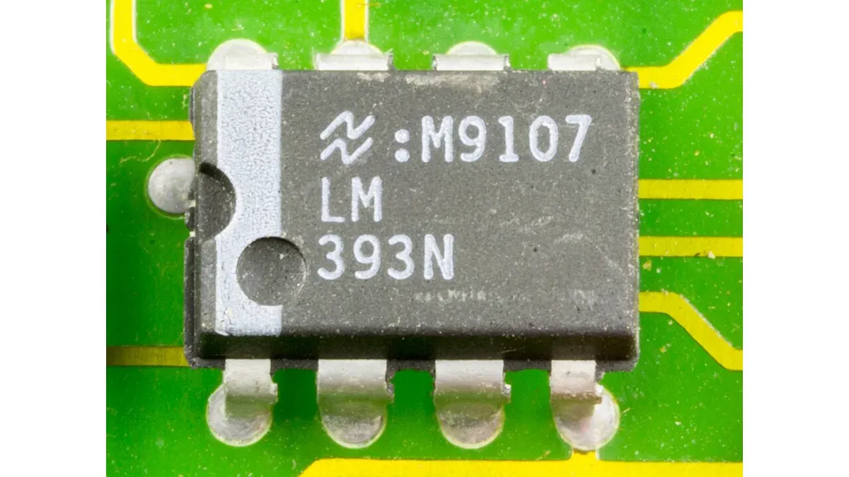
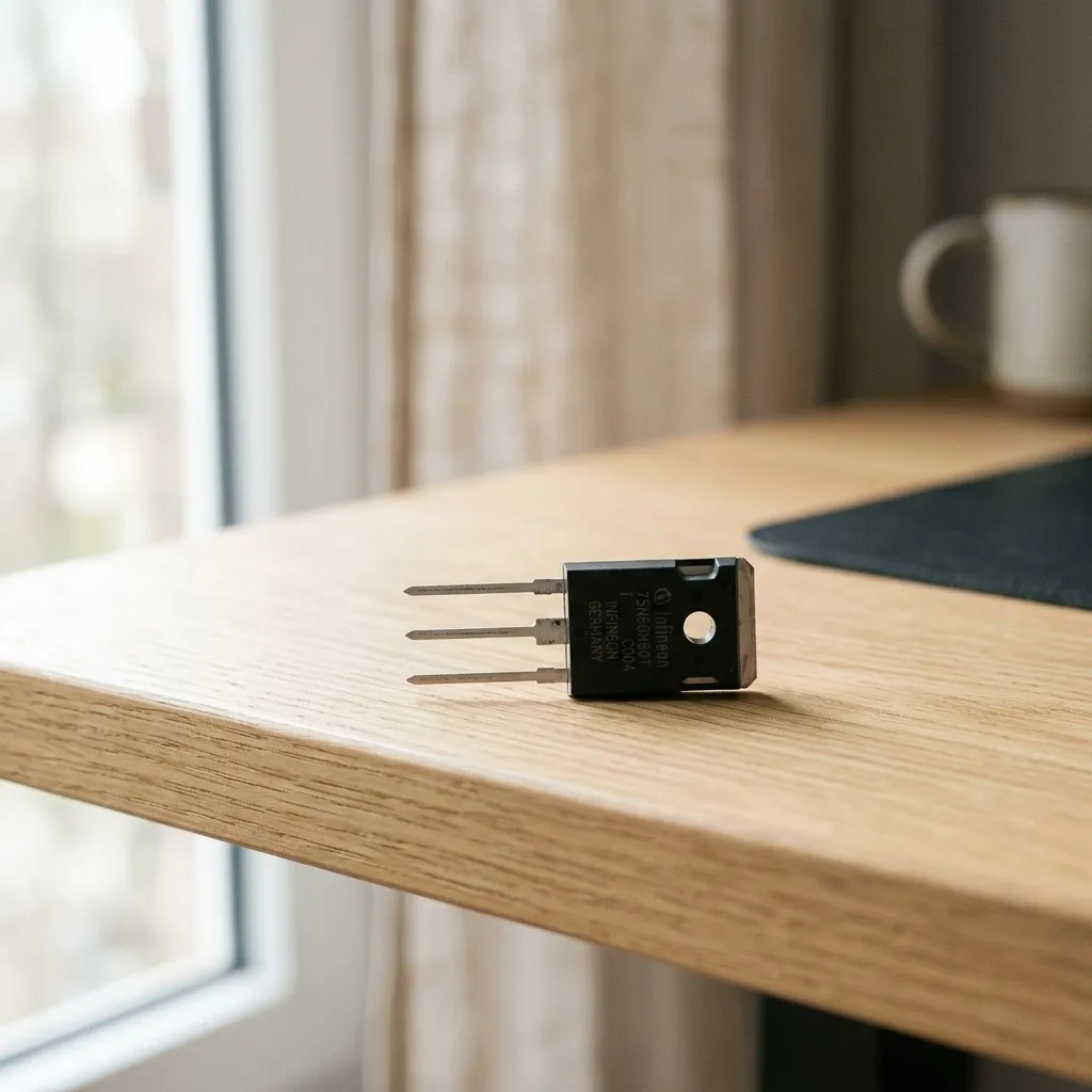
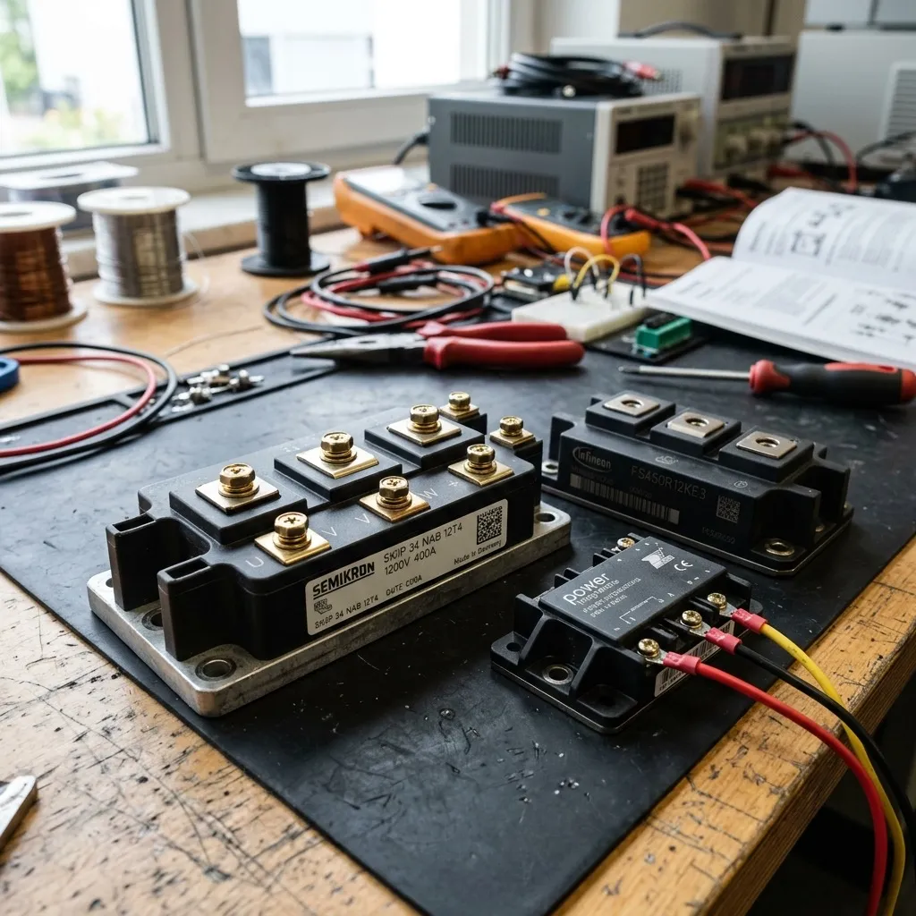 Fig 1: Silicon carbide (SiC) MOSFETs and gallium nitride (GaN) HEMTs in AI data center power delivery architectures. 800V HVDC rack distribution demands WBG semiconductors at the front-end and point-of-load stages.
NVIDIA and Google: First Deployments, Q3 2026
The 800V HVDC transition is not theoretical—it’s shipping. TrendForce reported on June 15, 2026 that NVIDIA (in partnership with Delta Electronics) and Google (in partnership with Flex) are deploying first-generation 800V HVDC racks in Q3 2026.
NVIDIA + Delta Electronics: Delta’s 800V HVDC power shelf, designed specifically for NVIDIA’s GB200 NVL72 rack-scale system, delivers 150kW per rack with 97.5% end-to-end power conversion efficiency. Each shelf contains 12x 12.5kW power modules using Infineon CoolSiC 1200V MOSFETs for the AC-DC front-end and CoolGaN 650V HEMTs for the intermediate bus conversion. The estimated SiC and GaN semiconductor content per rack is approximately $18,000-22,000 at current pricing.
Google + Flex: Google’s 800V HVDC architecture, developed for its in-house TPUv6 AI accelerator racks, uses a mixed-supplier approach: Wolfspeed SiC MOSFETs for the 800V AC-DC front end (Google has publicly disclosed its SiC supplier qualification in OCP Summit presentations) and EPC eGaN FETs for the 48V-to-1V point-of-load VRMs, where EPC’s chip-scale packaging (no plastic overmold, direct solder-bump connection) provides lower parasitic inductance for the nanosecond-scale transient response that TPU workloads demand.
For procurement, the significance of these first deployments is that they will consume incremental SiC and GaN capacity that was not in the 2025 supply forecast. The Delta and Flex power shelf programs alone are expected to consume an estimated 5-8% of global 1200V SiC MOSFET capacity in 2026—capacity that would otherwise have been available for automotive and industrial customers.
Supply Chain Constraints: The Packaging Bottleneck
The SiC substrate shortage—the constraint that defined the market from 2020-2024—is easing. Wolfspeed’s Siler City 200mm fab, ST’s Catania 200mm campus, and Chinese substrate suppliers (Sanan, TankeBlue, SICC) have collectively doubled global SiC substrate capacity since 2023.
The new constraint is advanced packaging for power modules:
-
Silver sintering for die attach—required for SiC modules operating at 200°C junction temperature—has limited equipment availability. The sintering press suppliers (ASM Pacific, Besi, Kulicke & Soffa) cannot deliver machines fast enough to meet the combined automotive and data center demand ramp.
-
Advanced ceramic substrates—Si₃N₄ (silicon nitride) replacing Al₂O₃ (alumina) for higher thermal conductivity and mechanical reliability—are in tight supply. Only Toshiba Materials, Denka, and Rogers Corporation produce Si₃N₄ substrates at the quality level required for automotive-and data-center-grade power modules.
-
Copper ribbon bonding replacing aluminum wire bonds—required for the higher current density and improved thermal cycling reliability of SiC power modules—uses specialized equipment that is also in high demand from the automotive traction inverter market.
The practical consequence: SiC MOSFET die availability is not the bottleneck. You can get SiC die. The bottleneck is getting those die assembled into qualified, reliable power modules in the volumes that AI data center deployments require.
Procurement Implications: 4 Actions for Power Semiconductor Buyers
1. Segment Your SiC Demand by Application Criticality
If you are buying SiC MOSFETs for automotive traction inverters, you are competing with data center PSU manufacturers for the same 1200V SiC MOSFET capacity. This was not true in 2024; it is true in 2026. Automotive buyers who previously enjoyed priority allocation—because automotive was the only volume SiC market—now face competition from data center programs that have comparable volume and, in some cases, higher willingness to pay.
Action: Classify your SiC BOM into “lifetime-buy qualified” (cannot be redesigned), “dual-source qualified” (second source already validated), and “new design” (can select supplier based on allocation availability). Prioritize allocation commitments for the first category.
2. Qualify GaN for Non-Isolated DC-DC Where Possible
For 48V-to-12V and 48V-to-1V conversion stages where galvanic isolation is not required, GaN HEMTs offer shorter lead times and more supplier options than SiC MOSFETs. GaN-on-Si is fabricated on existing 200mm and 300mm silicon CMOS lines; the manufacturing infrastructure is significantly more elastic than SiC’s specialized crystal growth and high-temperature processing.
If your power supply design currently uses SiC for non-isolated DC-DC stages, evaluate whether GaN can replace it—the lead time and supply elasticity benefits are meaningful, and the performance is at least equivalent for sub-650V, sub-100kHz applications.
3. Engage Power Module Integrators Early
If you are not a power module designer yourself—if you buy power shelves or power supplies from Delta, Flex, Artesyn, or Bel Power—your SiC and GaN supply chain exposure is indirect (through your PSU supplier’s semiconductor procurement). But that does not mean you should be passive.
Action: Ask your PSU suppliers what SiC and GaN suppliers they have qualified, whether they have dual-source strategies for the critical WBG devices in your power shelf, and what their allocation status is with their primary semiconductor suppliers. If the answer is “single-sourced and no allocation concern”—verify that. Data center PSU demand is growing faster than the WBG supply base, and allocation conflicts are emerging.
4. Monitor Innoscience and Chinese GaN Suppliers—Carefully
Innoscience has the lowest GaN HEMT pricing in the industry (approximately 30-40% below Infineon/Navitas equivalents) and the shortest lead times (8-12 weeks). For non-defense, non-government, non-critical infrastructure applications, Innoscience GaN FETs represent a genuinely compelling cost-reduction opportunity.
The caution: Innoscience is a Chinese company, and GaN HEMTs are on the BIS emerging technology control list. For applications subject to U.S. export controls, government procurement regulations, or entity-list restrictions, Innoscience devices may not be usable regardless of their technical or commercial merits.
SupplyICs tracks wide-bandgap semiconductor supply and pricing across all major SiC and GaN manufacturers. Our power electronics procurement desk can provide same-day availability checks on specific Wolfspeed, Infineon, ST, onsemi, Navitas, EPC, and TI part numbers. Contact us for your WBG semiconductor requirements or upload your BOM for a comprehensive supply risk analysis.
Frequently Asked Questions (FAQ)
Why are AI data centers switching from 48V to 800V HVDC power distribution?
A single NVIDIA B200 GPU rack in 2026 consumes approximately 120kW—roughly 10x the power density of a traditional server rack from 2020. Delivering that power at 48V requires copper bus bars the size of your forearm and generates unacceptable I²R losses. 800V HVDC (High-Voltage Direct Current) distribution reduces current by a factor of ~17x for the same power, dramatically shrinking bus bar size and distribution losses. The trade-off is that 800V-to-1V point-of-load conversion requires wide-bandgap semiconductors—SiC MOSFETs for the 800V-to-48V front-end and GaN HEMTs for 48V-to-1V GPU core voltage regulation—because silicon MOSFETs cannot switch efficiently at the required voltage and frequency combinations.
Who are the leading suppliers for SiC and GaN devices in AI data center power applications in 2026?
Gartner named Infineon Technologies as the market leader for AI data center power semiconductors in June 2026, citing its combined SiC MOSFET (CoolSiC) and GaN HEMT (CoolGaN) portfolio. For SiC specifically: Wolfspeed leads in substrate and device capacity; STMicroelectronics has the most vertically integrated SiC supply chain; onsemi's EliteSiC family is strong in server PSU applications. For GaN: Navitas Semiconductor and EPC (Efficient Power Conversion) are the pure-play leaders; Infineon and Texas Instruments offer GaN integrated with drivers/controllers; Innoscience (China) is the volume/cost leader for commodity GaN FETs but faces export control sensitivity for AI infrastructure applications.
What are the lead times and supply constraints for SiC and GaN devices in 2026?
SiC MOSFET lead times are 26-40 weeks for automotive and industrial qualified devices, driven not by wafer capacity (200mm production has alleviated the substrate bottleneck) but by module packaging capacity—silver sintering, advanced ceramic substrates, and copper ribbon bonding capabilities are the new constraint. GaN HEMT lead times are shorter at 12-20 weeks, reflecting GaN-on-Si fabrication using existing 200mm CMOS infrastructure that provides more manufacturing elasticity. The critical supply risk is that AI data center demand for both device categories is additive to existing automotive and industrial demand, which is also growing—creating potential allocation conflicts in H2 2026 as AI power supply volumes ramp.