Advanced Packaging Constraints in 2026: CoWoS Bottlenecks and AI Logic Chips
Table of Contents
⚡ Sourcing Summary
TSMC's CoWoS (Chip-on-Wafer-on-Substrate) advanced packaging is the primary bottleneck for AI logic chips in 2026. Sourcing teams must monitor interposer capacities and explore alternative multi-die packaging platforms to prevent high-performance compute delays.
If you track the semiconductor supply chain in 2026, you will quickly notice a paradigm shift. For decades, Moore’s Law dictated that the primary chokepoint in chip manufacturing was shrinking the transistor on the silicon wafer. Today, the foundries can produce 3nm and 2nm logic dies with relatively high yields.
The true bottleneck preventing hyperscalers from deploying AI data centers at their desired speed is no longer the silicon fabrication itself—it is Advanced Packaging. Specifically, the 2.5D and 3D packaging technologies required to connect high-performance logic chips with High Bandwidth Memory (HBM).
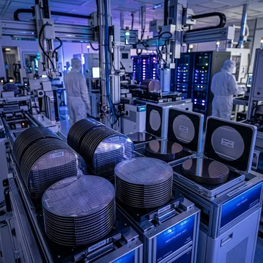
The Rise of CoWoS
At the heart of the AI hardware boom is TSMC’s Chip-on-Wafer-on-Substrate (CoWoS) technology. High-end AI accelerators from Nvidia, AMD, and custom ASIC designers rely entirely on CoWoS or equivalent 2.5D packaging.
Why is CoWoS Necessary?
Traditional organic substrates cannot support the microscopic interconnect densities required to link a massive GPU logic die to surrounding HBM stacks. CoWoS solves this by placing the chips on a silicon interposer, which acts as a microscopic bridge, allowing terabytes of data to flow between the logic and memory per second with minimal latency and power consumption.
The 2026 Capacity Crunch
Despite aggressive capital expenditure and rapid facility expansion by TSMC, Amkor, and Intel Foundry Services, advanced packaging capacity remains heavily allocated throughout 2026. Setting up a new packaging facility requires specialized equipment—such as ultra-precise pick-and-place machines and advanced thermal compression bonders—which themselves suffer from 12-to-18-month lead times.
How Packaging Bottlenecks Impact Global Procurement
For procurement professionals dealing with electronic components, the CoWoS bottleneck creates a profound ripple effect across the entire BOM (Bill of Materials).
- The “Golden Screw” Problem: You cannot ship a $400,000 AI server rack without the primary accelerator. Consequently, OEMs are hoarding peripheral components (PMICs, voltage regulators, high-speed networking switches) while waiting for their GPU allocations. This artificial hoarding occasionally causes unexpected spot shortages in otherwise unconstrained commodity components.
- Chiplet Architectures Driving Complexity: To bypass reticle limits, manufacturers are heavily adopting “chiplet” designs. Instead of one massive monolithic die, they manufacture smaller dies and package them together. This drastically improves silicon yield but exponential increases the demand for advanced packaging, exacerbating the capacity crunch.
SupplyICs Market Intelligence
Our market intelligence indicates that relief for the advanced packaging bottleneck will be gradual. While TSMC has successfully integrated new packaging plants in Taiwan and Japan, the insatiable demand from Generative AI and automotive ADAS (Advanced Driver Assistance Systems) continually outpaces the new supply.
For buyers, the strategy is clear: visibility into the upstream manufacturing constraints of your tier-1 components is essential. Understanding whether your critical logic chip uses standard flip-chip BGA or requires 2.5D interposer packaging allows you to accurately forecast lead times and adjust your safety stock of peripheral components accordingly.
Navigating supply chain delays driven by advanced packaging shortages? SupplyICs leverages deep market intelligence and a global inventory network to help you source critical networking and logic components.
References & Sources
- JEDEC Solid State Technology Association - Standards for Semiconductor Packing and MSL Traceability (J-STD-020 & J-STD-033).
- Automotive Electronics Council (AEC) - AEC-Q100 Stress Test Qualification for Integrated Circuits.
- TSMC - Advanced Packaging Technology Documentation (2026).
- Semiconductor Industry Association (SIA) - 2026 State of the Global Semiconductor Supply Chain.
SupplyICs Sourcing Team
Contact Our TeamIndependent Component Specialists
A team of veteran buyers navigating the global spot market. We specialize in locating hard-to-find, shortage, and EOL components. From strict anti-counterfeit verification to cross-reference matching, we provide frontline data to help you secure authentic stock safely.