Table of Contents
A crystal is not a drop-in frequency label. In a microcontroller Pierce oscillator, the crystal, internal inverter, external capacitors, board parasitics, bias network, and layout form one analog loop. A substitution that matches frequency and package can still start slowly, run off frequency, or exceed the crystal’s drive rating.
This guide is for board-level crystal selection. It does not cover integrated TCXO, OCXO, or MEMS oscillator modules, which are addressed in the precision oscillator sourcing guide.
How do you calculate load capacitors for a Pierce crystal oscillator?
Choose the two external capacitors so their series combination plus estimated board and pin stray capacitance matches the crystal’s specified load capacitance. For a common Pierce network, the starting relationship is:
CL ≈ (C1 × C2) / (C1 + C2) + Cstray
When C1 equals C2, the series term is approximately half either capacitor. Cstray includes MCU pin capacitance, package capacitance, traces, pads, and other coupling. It is a board-specific estimate, not a universal number to copy from an application note.
STMicroelectronics AN2867, accessed September 24, 2026, treats load capacitance, gain margin, drive level, and layout as linked oscillator-design variables. Use the exact MCU oscillator specification because internal transconductance and pin capacitance differ between families and operating modes.
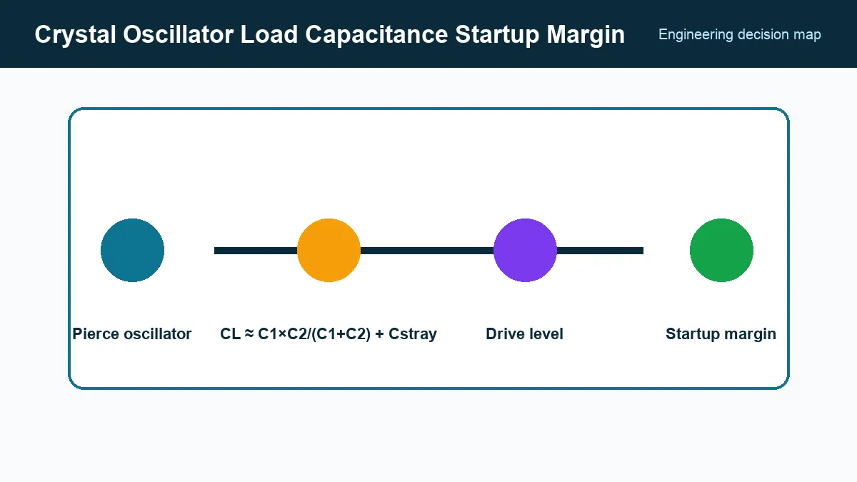
A crystal specified at 8 pF and one specified at 12.5 pF are not interchangeable merely because both say 16 MHz. With the same board capacitors, they see different load error and therefore different frequency pulling. Capture the specified CL, tolerance, equivalent series resistance (ESR), shunt capacitance, drive level, operating mode, temperature range, package, and aging limit in the approved part record.
Why can increasing oscillator drive reduce crystal reliability?
Increasing oscillator gain or reducing damping can improve startup while pushing crystal current above the resonator’s drive rating. Excess drive can shift frequency, accelerate aging, or damage the crystal. Check the crystal manufacturer’s limit and the MCU oscillator’s available drive before changing gain or resistance.
The accurate way to determine drive is the method recommended by the MCU and crystal vendors, often using a current measurement arrangement and the crystal’s motional parameters. A normal oscilloscope probe placed directly on an oscillator node can add enough capacitance to change the condition being measured.
Start with the MCU vendor’s recommended network, then calculate and measure rather than tuning for the largest visible waveform. A clipped waveform is not evidence of adequate oscillator margin.
How do you verify crystal startup margin on the production board?
Verify that the oscillator’s negative-resistance magnitude exceeds the crystal’s worst-case equivalent series resistance (ESR) by the margin required by the MCU or crystal vendor, then measure startup across the production conditions. NXP AN14518, accessed September 24, 2026, describes how capacitance, startup, and gain margin interact during oscillator characterization.
A practical validation inserts a known series resistance and identifies where startup ceases under controlled conditions. The result can be used with the circuit model to estimate available negative resistance. Apply the manufacturer’s method rather than treating one resistor value as a universal pass limit.
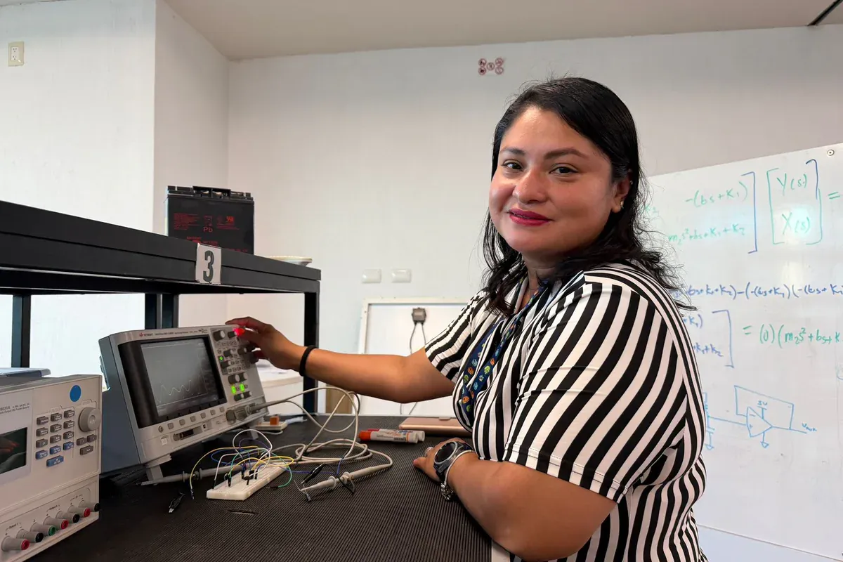
Test cold, room, and hot conditions; supply extremes; the slowest permitted supply ramp; and multiple crystals from representative lots. Record startup time from the relevant reset or enable event. A design that starts after several seconds during a lab power cycle may violate the firmware’s clock-failure window even if steady-state frequency is correct.
Layout is part of the oscillator component
Keep the crystal and load capacitors close to the MCU oscillator pins, minimize loop area, and avoid routing fast clocks or high-current switching nodes through the oscillator region. Give each capacitor a short ground return consistent with the reference layout.
Guarding, ground placement, and unused copper should follow the MCU vendor’s guidance. Adding a ground plane directly beneath every crystal is not automatically beneficial because it can increase stray capacitance. Flux residue and moisture can also add leakage around high-impedance nodes.
Do not approve a substitute only on an evaluation board if the production PCB has different layer construction, trace geometry, or nearby switching activity. The approved result belongs to a crystal, capacitor values, MCU revision, oscillator mode, and PCB revision together.
Release a measurable oscillator specification
The purchase specification should identify full ordering code, frequency, CL, ESR maximum, drive-level maximum, stability/tolerance budget, temperature range, package, and lifecycle status. Engineering release should add the validated capacitor values, any damping resistor, startup limit, negative-resistance method, and test conditions.
For incoming substitutions, compare those fields before samples reach assembly. The final release evidence should include frequency at the chosen measurement point, startup distribution across conditions, and confirmation that measurement loading was controlled. That makes the oscillator a qualified circuit rather than a nominal-frequency guess.
Frequently Asked Questions (FAQ)
Should the two external crystal capacitors equal the crystal load capacitance?
Usually no. For equal capacitors, their series combination is about half either capacitor, and board plus pin stray capacitance must also be included. Use the oscillator vendor's model and confirm the result by measuring frequency on the assembled board.
Can a crystal with a lower load-capacitance rating replace the original?
Only after recalculating the external network and verifying frequency error, drive level, startup, and loop margin. Keeping the old capacitors can pull the new crystal away from its specified load condition.
Why can an oscillator work on the bench but fail in production?
A marginal loop may start only with favorable crystal motional resistance, temperature, supply ramp, contamination, or probe loading. Production validation should cover worst-case component limits and environmental conditions.