Advanced Counterfeit Detection and Component Authentication: The 2026 Testing Standards Guide for High-Reliability Electronics
Table of Contents
- The 2026 Counterfeit Threat Landscape
- The Testing Hierarchy: Risk-Based Authentication
- Test Method 1: External Visual Inspection and Documentation Review
- Test Method 2: X-Ray Inspection (Real-Time Radiography)
- Test Method 3: Scanning Acoustic Microscopy (SAM)
- Test Method 4: X-Ray Fluorescence (XRF) Material Analysis
- Test Method 5: Electrical Verification
- Test Method 6: Decapsulation and Die Analysis
- Building an In-House Authentication Capability
- Industry Collaboration and Reporting
- Conclusion
- References & Sources
⚡ Sourcing Summary
Counterfeit semiconductor detection requires an uncompromising quality assurance program in 2026. Audit protocols must include high-magnification optical inspection, X-ray lead frame analysis, decapsulation, and curve tracer parametric testing.
In March 2026, the U.S. Department of Defense reported that counterfeit electronic components had been detected in the supply chains of 17 separate defense acquisition programs over the preceding 12 months—the highest annual count since the Senate Armed Services Committee investigation of 2011 first brought the issue to national attention. The counterfeiters’ methods have evolved. Optical inspection alone, once the frontline defense, now catches only approximately 60% of professionally produced counterfeit components.
The sophistication of modern counterfeiting demands a correspondingly sophisticated detection capability. This guide provides a technical reference for procurement and quality professionals who need to understand—and verify—that their component authentication protocols meet the threat landscape of 2026.
The 2026 Counterfeit Threat Landscape
Understanding the detection challenge requires understanding what you are detecting. Modern electronic component counterfeiting encompasses several distinct categories:
| Counterfeit Type | Description | Detection Difficulty |
|---|---|---|
| Remarked / Blacktopped | Used or lower-grade parts with surface coating and new laser marking applied to appear as higher-spec, newer date code, or military/automotive grade | Medium |
| Refurbished / Pulls | Used components removed from discarded equipment, cleaned, re-tinned, and sold as “new original” | Medium-High |
| Die Swap / Package Fraud | Authentic package containing a different, lower-specification die; or a commercial-grade die in a package marked as extended-temperature or MIL-SPEC | High |
| Empty / Dummy Package | Package with no functional die inside; may contain a non-functional placeholder to provide weight and appearance of authenticity | Medium |
| Cloned / Fake Silicon | Components manufactured by an unauthorized third party using stolen or reverse-engineered mask sets | Very High |
| Factory Rejects / Floor Sweepings | Genuine parts that failed the manufacturer’s outgoing quality tests, scraped from factory waste streams and resold | High |
A comprehensive authentication protocol must be capable of detecting all categories. No single test method is sufficient.
The Testing Hierarchy: Risk-Based Authentication
Resources for component authentication are always finite—you cannot X-ray, decapsulate, and electrically test every resistor in every incoming shipment. A risk-based approach aligns testing depth with the consequences of failure:
| Risk Level | Component Profile | Testing Protocol | Example Components |
|---|---|---|---|
| Level 1 — Low | Commercial grade, low value, non-critical function, franchised source | Visual inspection + documentation review | Consumer passives, LED drivers, commodity connectors |
| Level 2 — Medium | Industrial grade, moderate value, important function, independent source | Level 1 + X-ray + solderability + marking permanency | Industrial MCUs, power MOSFETs, precision op-amps |
| Level 3 — High | AEC-Q100, high value, critical function, open market source | Level 2 + SAM + electrical verification + XRF | Automotive MCUs, FPGA/CPLD, isolated gate drivers |
| Level 4 — Critical | MIL-STD / space-grade / medical, very high value, safety-critical, any non-authorized source | Level 3 + decapsulation + full parametric test + burn-in | MIL-STD FPGAs, rad-hard ICs, implantable medical ASICs |
This framework aligns with SAE AS6081 (Counterfeit Electronic Parts; Avoidance, Detection, Mitigation, and Disposition) and IDEA-STD-1010 (Acceptability of Electronic Components), the two primary standards governing electronic component authentication in the independent distribution channel.
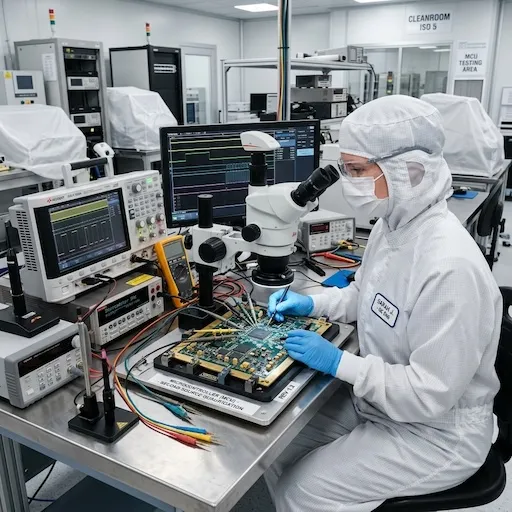
Test Method 1: External Visual Inspection and Documentation Review
External visual inspection (EVI) is the first line of defense—and the most commonly bypassed by sophisticated counterfeiters. Nevertheless, properly executed EVI catches a meaningful percentage of counterfeits and is essential as a screening step.
Equipment Requirements:
- Stereo zoom microscope: 10x–60x minimum magnification, with coaxial and oblique lighting
- Digital microscope with image capture: 50x–200x for detailed marking and lead/solder ball inspection
- UV light source (365nm): For detecting surface coating anomalies, rework residues, and blacktopping compounds
- Calibrated digital calipers and micrometer: For package dimensional verification against manufacturer mechanical drawings
Inspection Points (per IDEA-STD-1010):
-
Marking Permanency: Apply specified solvent (per MIL-STD-883 Method 2015 or manufacturer specification) to device markings. Counterfeit markings often dissolve, smear, or detach. Always reference the OCM’s specification for the specific device and date code, as different manufacturers use different marking ink formulations.
-
Marking Consistency: Compare the font, character spacing, logo geometry, pin-1 indicator style, and text alignment against a known-good reference sample or the OCM’s marking specification. Laser-etched markings on counterfeit parts frequently show differences in dot pitch, depth uniformity, and edge definition when examined at 100x+ magnification.
-
Package Surface and Molding Compound: Under oblique lighting at 20x–40x, examine for surface texture inconsistencies suggesting resurfacing or blacktopping, sanding marks or mechanical abrasion, chemical etching residue or discoloration, uneven mold compound color, and evidence of previous solder on leads that have been re-tinned.
-
Lead/Solder Ball Condition: Examine for non-uniform lead plating thickness or color, evidence of straightening (bent leads re-straightened leave micro-cracks visible at 30x+), excess solder on BGA balls suggesting reballing, and oxidation, pitting, or intermetallic growth on terminations indicating prior use.
-
Documentation Cross-Verification: Cross-reference all supplied documentation against manufacturer-verifiable records. Verify that date codes, lot codes, and country of origin are consistent across documentation, external packaging, inner packaging, and the components themselves.
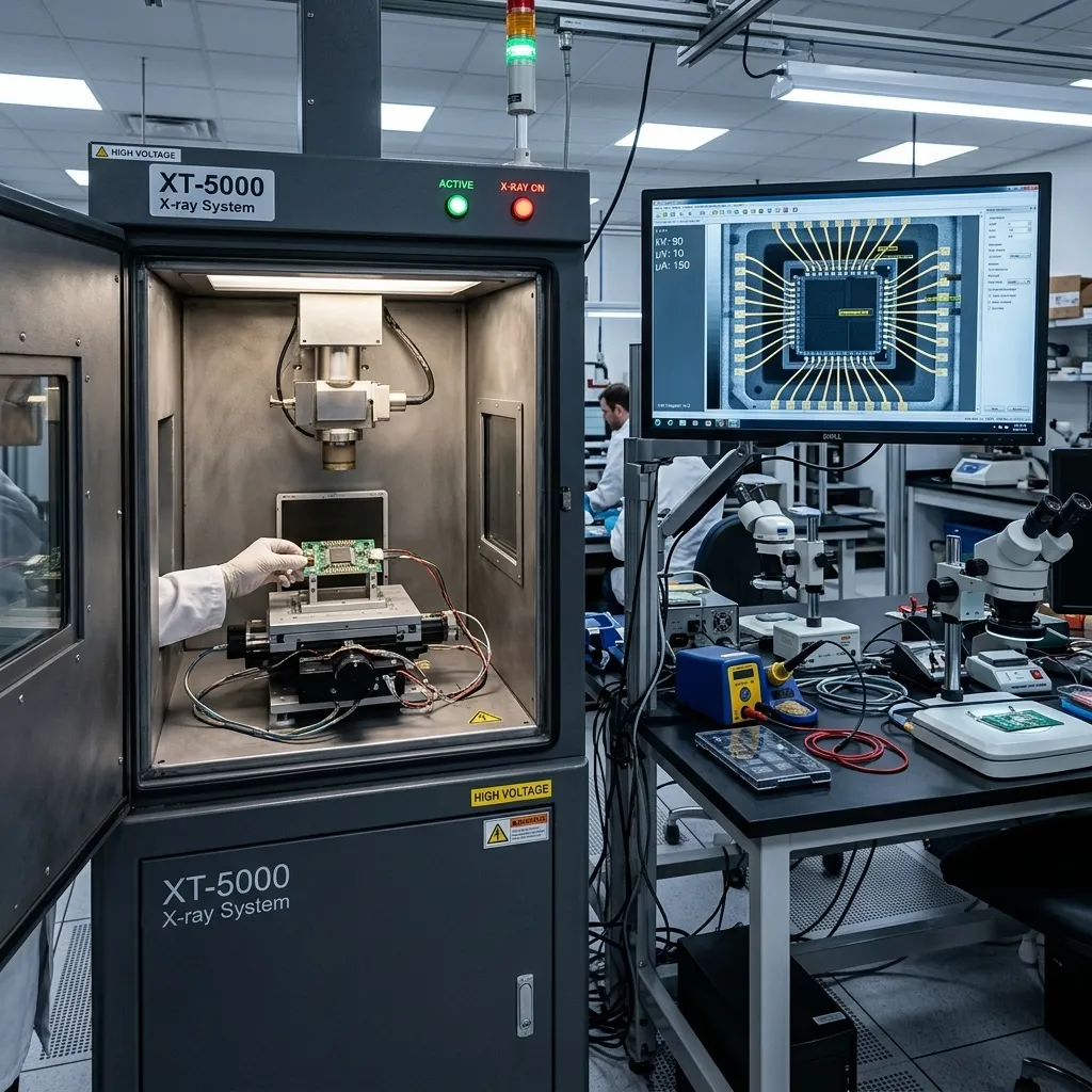
Test Method 2: X-Ray Inspection (Real-Time Radiography)
X-ray inspection provides non-destructive visibility into the internal structure of a component. It is the single most valuable screening tool for detecting die-swap, empty-package, and internal construction anomalies.
Equipment Requirements:
- Real-time microfocus X-ray system: <1 μm focal spot size, 90–160 kV tube voltage range
- Digital detector: 16-bit minimum, with geometric magnification capability
- Image processing software: Contrast enhancement, measurement tools, image overlay/comparison
Inspection Points:
-
Die Size and Orientation: Measure the X-ray image of the internal die against the manufacturer’s known die dimensions (available from die databases, authorized distributor documentation, or destructive analysis of a known-good sample). A smaller die than specified is the hallmark of a remarked lower-specification part.
-
Wire Bond Count and Pattern: Count the number of wire bonds and verify the bonding pattern against a known-good reference. Missing wire bonds, inconsistent loop heights, or different bond pad locations are critical red flags. Copper wire bonds (increasingly used for cost reduction in commercial parts) have different X-ray contrast than gold wire bonds—a difference counterfeiters cannot easily hide.
-
Die Attach and Leadframe: Verify that the die attach paddle, leadframe design, and internal construction match the manufacturer’s specification. Counterfeiters cannot economically replicate custom leadframes, so deviations from expected internal structure are highly diagnostic.
-
Die Surface Markings: At maximum magnification and appropriate kV settings, some die surface markings (manufacturer logo, part number abbreviation, die revision) may be visible on X-ray. These should match the external package markings. A mismatch is definitive evidence of fraud.
-
Internal Voids and Anomalies: X-ray reveals internal voids, delamination between die and die attach, and anomalies in the molding compound that indicate rework or poor-quality counterfeit manufacturing.
X-ray inspection equipment has become significantly more accessible. Benchtop microfocus X-ray systems suitable for component inspection are now available in the $50,000–$80,000 range, and the technology has become a standard fixture in qualified independent distributors’ quality laboratories.
Test Method 3: Scanning Acoustic Microscopy (SAM)
While X-ray reveals density variations, Scanning Acoustic Microscopy (SAM) reveals interfaces. SAM uses ultrasonic waves to detect delamination, voids, and cracks at material interfaces invisible to both optical inspection and X-ray.
Equipment Requirements:
- Scanning Acoustic Microscope: 15–230 MHz transducer range; C-SAM (C-mode) is standard for component inspection
- Immersion medium: Deionized water or inert fluid
- Reference standards: Known-good samples of the same device type
Key Detection Capabilities:
-
Die Attach Delamination: SAM is uniquely capable of detecting delamination between the silicon die and the die attach paddle—common in used/refurbished parts that have undergone thermal cycling and extremely difficult to detect through any other non-destructive method.
-
Molding Compound Delamination: The “halo” pattern characteristic of molding compound separation from the leadframe or die surface indicates either prior thermal stress (used parts) or poor-quality re-molding (counterfeit).
-
Package Crack Detection: Micro-cracks in the package body, often invisible to optical inspection, are clearly resolved by SAM. These cracks can allow moisture ingress leading to field failures through corrosion or popcorn cracking during reflow soldering.
-
Substrate and Interposer Integrity: For BGAs, CSPs, and advanced packages, SAM evaluates substrate and interposer layer integrity. Delamination here can cause latent opens in the solder ball-to-substrate interface.
SAM is particularly important for automotive, military, and medical components that will experience thermal cycling in service. A component with die attach delamination may pass room-temperature electrical testing but fail after 500 thermal cycles in an engine compartment or avionics bay.
Test Method 4: X-Ray Fluorescence (XRF) Material Analysis
XRF provides non-destructive elemental analysis of component materials. It is the primary tool for verifying RoHS compliance and detecting material substitution—a common counterfeit technique where lead-free terminations are replaced with cheaper tin-lead plating.
Equipment Requirements:
- Benchtop or handheld XRF analyzer with semiconductor detector
- Calibration standards for RoHS elements (Pb, Hg, Cd, Cr-VI, Br) and common alloy compositions
- Spot size appropriate for termination geometry (typically 0.1–3 mm)
Inspection Points:
-
Termination Finish Composition: Verify measured termination plating composition matches manufacturer specification. For RoHS-compliant parts, verify lead content below 1000 ppm. A part marked RoHS-compliant measuring 5%+ lead is fraudulently labeled.
-
Leadframe Base Material: Different manufacturers use specific copper alloy formulations (e.g., C19400, C70250, EFTEC-64T). XRF detects substitution of cheaper alloys.
-
Molding Compound Fillers: Semiconductor molding compounds contain specific silica filler loading percentages. Deviations from expected composition suggest re-molding.
-
Bond Wire Material Indication: While XRF cannot isolate individual bond wires, bulk analysis detects whether gold, copper, or palladium-coated copper (PCC) wire bonds are present. A manufacturer using gold wire bonds exclusively should not have copper present in bulk XRF spectrum.
XRF is rapid (30–120 seconds per measurement), non-destructive, and requires minimal operator training. It should be part of every incoming inspection protocol for open market components.
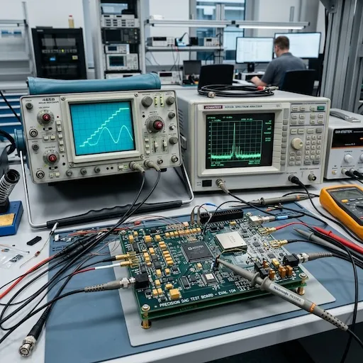
Test Method 5: Electrical Verification
Visual, X-ray, SAM, and XRF analysis can all be passed by a component that is structurally authentic but electrically defective. Electrical verification closes this gap.
Equipment Requirements:
- Source Measurement Unit (SMU) or semiconductor parameter analyzer
- Curve tracer for basic I-V characterization
- Functional test platform for digital components
- Environmental chamber for temperature-dependent verification
Inspection Points:
-
Pin-to-Pin I-V Curve Analysis: Every semiconductor device has a characteristic current-voltage signature on each pin pair. A curve tracer compares these signatures against a known-good “golden device” reference. Deviations in I-V characteristics—opens, shorts, leakage currents, or different breakdown voltages—indicate a different die, ESD damage, or electrical degradation from prior use.
-
Key Parametric Verification: For active components, verify critical datasheet parameters: supply current (active and standby) at nominal Vcc, input leakage current, output drive capability at specified current levels, oscillator startup and frequency, and power-on reset threshold.
-
Temperature-Dependent Testing: Counterfeit components often pass room-temperature parametric testing but fail at temperature extremes. For Level 3 and 4 risk components, verify key parameters at both cold (-40°C or -55°C) and hot (+125°C or +150°C) conditions. Used components with degraded die attach show parametric shifts under thermal stress that factory-fresh components will not.
-
ID Code and Register Verification: For microcontrollers, FPGAs from Xilinx/AMD and Intel/Altera, and other programmable devices, read the device ID register or JTAG ID code and verify it matches the expected value for the marked part number and silicon revision. This single test catches a large fraction of remarked devices—counterfeiters cannot change silicon-level identification registers.
-
Functional Pattern Testing: For the highest-risk components, apply a functional test pattern exercising critical datapaths, memory interfaces, and I/O blocks. The test does not need 100% fault coverage; a targeted pattern typically catches manufacturing defects and degraded silicon.
Test Method 6: Decapsulation and Die Analysis
Decapsulation (decap) is destructive—the component cannot be used afterward—but it provides the highest confidence in authenticity for critical procurements.
Equipment and Methods:
- Chemical decapsulation: Heated fuming nitric or sulfuric acid (automated jet etcher for production; manual drop method for low volume)
- Laser decapsulation: For copper wire bond devices where acid may attack bonds
- Post-decap inspection: High-magnification optical microscope (200x–1000x) or SEM
Inspection Points:
-
Die Markings: The silicon die carries manufacturer identification—logo, part number abbreviation, die revision code, and often fab/lot identifier etched into the top metal layer. These markings are extraordinarily difficult to forge. A mismatch between die markings and package markings is the gold standard for counterfeit identification.
-
Die Dimensions: Measure die dimensions and compare against manufacturer die database records or known-good reference. A smaller die than implied by package marking is definitive evidence of fraud.
-
Die Layout and Topology: Even without readable die markings, the arrangement of functional blocks, pad ring configuration, and number/position of bond pads creates a unique fingerprint. Comparison with known-good reference die photographs confirms authenticity or identifies substitution.
-
Process Technology Indicators: The process technology node (e.g., 180nm, 90nm, 28nm) is visible in feature size and structure. A part marked as a 28nm FPGA but containing a 130nm die is clearly fraudulent.
-
Bond Wire Material Verification: Direct SEM/EDS analysis of bond wires and pads identifies wire material (Au, Cu, PCC, Al) and detects intermetallic compounds indicating prior use or thermal stress.
Destructive analysis is performed on a sample basis (1-5 pieces per lot). For critical procurements, the cost of destroyed samples—even at hundreds of dollars each—is negligible compared to the cost of a single field failure.
Building an In-House Authentication Capability
For organizations with sufficient volume, building in-house authentication capability provides faster turnaround and greater control than relying entirely on external labs:
Phase 1 — Essential Screening (Investment: $30,000–$60,000)
- Digital microscope (20x–200x) with image capture: $5,000–$15,000
- UV inspection lamp and solvent test kit: $2,000
- Benchtop microfocus X-ray system: $25,000–$45,000
This combination catches approximately 85% of counterfeit components detectable through non-destructive methods.
Phase 2 — Enhanced Detection (Additional Investment: $80,000–$150,000)
- Handheld or benchtop XRF analyzer: $25,000–$40,000
- Semiconductor curve tracer: $15,000–$30,000
- Basic SAM capability or contracted SAM service access
This adds material verification and electrical screening, bringing non-destructive detection coverage to approximately 95%.
Phase 3 — Comprehensive Authentication (Additional Investment: $200,000+)
- Full parametric test capability (SMU, LCR meter, functional ATE)
- In-house SAM system: $100,000–$200,000
- Chemical decapsulation workstation with fume extraction: $20,000–$40,000
- Environmental chamber for temperature-dependent testing
Industry Collaboration and Reporting
Counterfeit detection is as much an information-sharing challenge as a technical one. When a procurement organization detects a counterfeit component, reporting to industry databases protects the entire supply chain:
- ERAI Incident Reporting: The central database for counterfeit electronic component incidents. Submitting a detailed report enables other organizations to identify and avoid the same counterfeit source.
- GIDEP (Government-Industry Data Exchange Program): For U.S. defense and aerospace supply chain participants, provides a secure platform for sharing counterfeit and non-conforming material alerts.
- CISA ICT Supply Chain Risk Management: For counterfeit incidents with national security implications, coordinates public-private information sharing.
Conclusion
In 2026, reliable electronic component authentication is the price of admission for any organization sourcing from the open market. The counterfeiters are well-funded, technically sophisticated, and incentivized by margins that can exceed 1000%. Basic visual inspection—still the most common authentication method in the industry—is decades out of date against the current threat.
A modern authentication protocol combines external visual inspection, X-ray radiography, material analysis (XRF), acoustic microscopy (SAM), electrical verification, and—for the highest-risk procurements—destructive die analysis. Coupled with rigorous supplier qualification practices, these testing protocols create a multi-layered defense that makes your supply chain a hard target rather than a soft one.
The cost of implementing these capabilities is real. The cost of not implementing them—measured in line stoppages, field failures, reputational damage, and in the worst case, safety incidents—is immeasurably higher.
SupplyICs operates a comprehensive component authentication laboratory equipped with digital microscopy, real-time microfocus X-ray, XRF material analysis, and semiconductor curve tracing. All components sourced through our network undergo risk-level-appropriate authentication testing before shipment. Components destined for military, aerospace, automotive, and medical applications are subject to enhanced authentication protocols. Contact our quality team to discuss your component authentication requirements.
References & Sources
- JEDEC Solid State Technology Association - Standards for Semiconductor Packing and MSL Traceability (J-STD-020 & J-STD-033).
- Automotive Electronics Council (AEC) - AEC-Q100 Stress Test Qualification for Integrated Circuits.
- SAE AS6081 — Counterfeit Electronic Parts; Avoidance, Detection, Mitigation, and Disposition — Distributors.
- IDEA-STD-1010 — Acceptability of Electronic Components Distributed in the Open Market.
- ERAI (Electronic Resellers Association International) — Counterfeit Component Incident Database and Reporting Standards.
- JEDEC JESD22 / J-STD-020 — Reliability Test Methods and Moisture/Reflow Sensitivity Classification.
- GIDEP (Government-Industry Data Exchange Program) — Counterfeit and Non-Conforming Material Alerts.
- CISA ICT Supply Chain Risk Management Task Force — Federal Guidance on ICT Supply Chain Security.
- U.S. Department of Defense — DFARS 252.246-7007: Counterfeit Electronic Part Detection and Avoidance.
SupplyICs Sourcing Team
Contact Our TeamIndependent Component Specialists
A team of veteran buyers navigating the global spot market. We specialize in locating hard-to-find, shortage, and EOL components. From strict anti-counterfeit verification to cross-reference matching, we provide frontline data to help you secure authentic stock safely.